
Every major AI accelerator shipped this year, from Nvidia's Blackwell GPUs to AMD's MI-series chips to Google's TPUs, contains a component that almost nobody outside the industry can name: a thin wafer of silicon that sits underneath the processor and its memory stacks, quietly moving terabytes of data per second. On October 8, GlobalFoundries announced a $2 billion, five-year manufacturing agreement with TSMC to produce exactly that component, the silicon interposer, at its Malta, New York facility. GlobalFoundries says the deal will create the first US-based source of silicon interposers for TSMC's CoWoS advanced packaging ecosystem, with volume production expected to begin ramping in the first half of 2028.
Shares of GlobalFoundries rose about 4 percent in premarket trading on the news, according to Reuters.
The Component That Runs the AI Boom
To understand why a $2 billion deal centers on something most people have never heard of, it helps to look inside an AI accelerator. Modern AI chips are not single monolithic dies. They are packages containing several dies sitting side by side: a large logic processor (a GPU or custom AI accelerator) flanked by multiple stacks of high-bandwidth memory, or HBM. The data highway connecting them cannot be an ordinary circuit board. HBM needs to shovel data to the processor at terabytes per second, and only a dense mesh of copper wiring measured in microns can carry that much traffic.
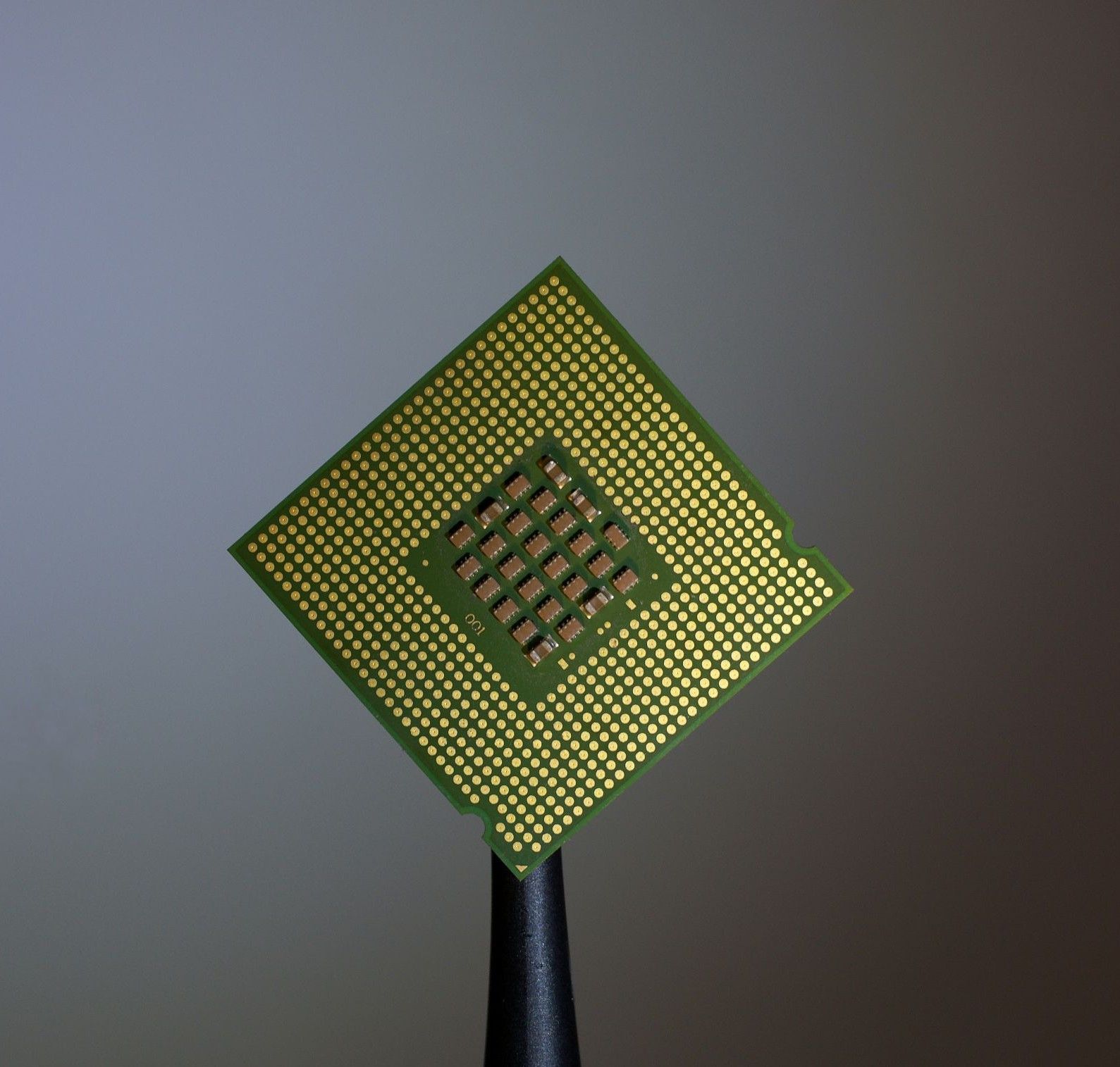
The silicon interposer is that highway. It is a piece of silicon wafer etched with fine-pitch copper wiring on its surface and pierced by thousands of through-silicon vias (TSVs), vertical copper-filled channels drilled through the silicon's full thickness that carry signals and power down to the package substrate. The wiring on top routes signals laterally between the GPU die and the HBM stacks, keeping paths so short and dense that the processor and memory effectively behave as one high-performance system. Without it, the memory bandwidth that AI training and inference demand cannot be delivered.
The agreement also covers embedded deep trench capacitors (DTCs), capacitors formed inside the silicon bulk of the interposer using deep trench etching. They suppress the voltage fluctuations that occur when a GPU suddenly draws large current spikes, a problem that has worsened as each accelerator generation draws more power. Power integrity at the interposer level is now an engineering constraint in its own right.
That explains why GlobalFoundries, a foundry, is doing this work at all. Interposers require front-end semiconductor processes: photolithography, copper wiring, deep trench etching, contamination control, yield management across large silicon areas. They are made at foundries, not at back-end assembly houses. Crucially, they do not require the leading-edge 3nm or 2nm transistors that TSMC and Samsung compete on. GlobalFoundries exited the sub-14nm transistor race in 2018 and rebuilt itself around specialty processes, which is why interposer manufacturing plays to its strengths.
The AI chip is no longer just the processor. It is the GPU, the memory, the silicon underneath, and the power delivery working as one system, and the silicon underneath has become scarce.
Why CoWoS Capacity Is the Real Constraint
Enjoying this story?
Get the five most important stories in tech, every morning. Free.
TSMC's CoWoS (Chip-on-Wafer-on-Substrate) packaging is the system this deal serves, and it has been the binding constraint on AI chip shipments for years. TSMC controls an estimated 90 percent of CoWoS-compatible advanced packaging capacity at AI-chip scale, and the company is targeting roughly 130,000 CoWoS wafer starts per month by late 2026, up from about 60,000 in early 2025. Yet analysts estimate the supply-demand gap remains around 20 percent even at that expanded scale, per TrendForce estimates cited in industry reporting.
The consequences are concrete. TSMC's CEO C.C. Wei has said publicly that CoWoS capacity is sold out through 2026. Nvidia holds approximately 60 percent of TSMC's available CoWoS allocation, per Morgan Stanley analysis cited across industry publications. Google reportedly cut its 2026 TPU production target from around 4 million units to roughly 3 million because of constrained CoWoS access. Intel CEO Lip-Bu Tan noted on the company's second-quarter 2026 earnings call that customers have been exploring its EMIB-T packaging technology as an alternative precisely because of this capacity squeeze.
That is the demand picture GlobalFoundries is selling into. Advanced packaging has shifted from a back-end afterthought to one of the central technologies of the AI boom, and the interposer sits at its center. Adding a second manufacturing node gives TSMC room to breathe at the exact choke point where its customers are rationed.
The 12,000-Mile Round Trip
The CoWoS Bottleneck in Numbers
Why a $2B interposer deal matters for AI chip supply
Sources: GF announcement (Oct 2026), Reuters, TrendForce and Morgan Stanley estimates via industry reporting.
The deal also addresses a geographic problem that has dogged US semiconductor policy. Chips fabricated at TSMC's Arizona fabs, built to reduce American dependence on Taiwan-based production, are currently shipped back to Taiwan for CoWoS packaging, a roughly 12,000-mile round trip that undercuts the supply security rationale for domestic wafer fabrication. The GlobalFoundries agreement closes one gap in that chain by putting interposer production on US soil, but not the biggest one.
Producing interposers in New York is not the same as completing CoWoS packaging in New York. The interposer is an upstream input to the full CoWoS process; TSMC's assembly lines, which bond the interposer to logic dies and HBM stacks, remain concentrated in Taiwan until additional US facilities come online. TSMC's Arizona packaging capability is targeted for "before 2029," per TSMC Deputy COO Kevin Zhang's comments earlier this year, and Amkor Technology is building a $2 billion advanced packaging facility in Peoria, Arizona, targeting early 2028 production. HBM memory, dominated by SK Hynix, Samsung, and Micron, has no US-based manufacturing at AI-chip scale at all.
So until Amkor Peoria and TSMC Arizona's packaging lines reach production, interposers made in Malta will still travel to Taiwan for final CoWoS assembly. The 12,000-mile problem is narrowed, not eliminated, before 2028.
What This Changes, and What It Does Not
The deal's significance is best read as strategic rather than immediate. Volume production ramps in the first half of 2028, so it does nothing for today's packaging shortage. But it locks in a piece of the next generation of AI infrastructure through an unusual partnership: TSMC, the world's dominant advanced foundry, is outsourcing a critical component to GlobalFoundries, a company it has historically regarded as a competitor.
One caveat: TSMC has not issued an independent statement confirming the deal. The news came entirely through GlobalFoundries' own press release and investor channels, so every detail so far traces to one side of the table.
Zooming out, the pattern is the story. In 2025, GlobalFoundries announced a $16 billion investment program across its New York and Vermont facilities, including a New York Advanced Packaging and Photonics Center dedicated to silicon photonics packaging. The interposer deal extends that push into the CoWoS ecosystem itself.
"Advanced packaging is becoming increasingly critical to delivering the performance, power efficiency and scale required for next-generation AI systems," said Ed Kaste, GlobalFoundries' senior vice president of CMOS Business, in the company's announcement. That is the thesis: the transistor race still matters, but the AI buildout is increasingly gated by the packaging that connects the pieces. A $2 billion bet on the silicon beneath the GPU is, in 2026, one of the most rational bets in semiconductors.
0 Comments