
The filing that made it official
This week, a Taiwanese government filing turned TSMC's most politically significant Japanese commitment into a dated engineering plan. The chipmaker's second fab in Kumamoto will begin mass production of 3-nanometer wafers in 2028, with a monthly capacity of 15,000 12-inch wafers. The filing confirms what chief executive C.C. Wei told Japanese Prime Minister Sanae Takaichi in a Tokyo meeting: the facility, originally designed for 6-to-12-nanometer output, will instead produce the world's most advanced logic process for AI workloads.
According to Japan's Yomiuri Shimbun, the upgrade lifts TSMC's investment in the second fab to $17 billion, up from $12.2 billion under the earlier, less ambitious plan. TSMC itself has not confirmed that figure, which is worth remembering: the number comes from Japanese media, not the company's balance sheet. What TSMC has confirmed, in Wei's own words, is the intent: "We believe this fab will further contribute to the local economic growth and, most importantly, form a foundation for Japan's AI business."
A reversal years in the making
Enjoying this story?
Get the five most important stories in tech, every morning. Free.
The Kumamoto site, operated through TSMC's JASM subsidiary, has had a winding road. TSMC first announced the second fab in February 2024 as part of a $20 billion planned investment in Japan. Then, in July 2025, construction was delayed so the company could prioritize expanding its manufacturing base in the United States. Wei publicly blamed excessive car traffic around the Kumamoto site, an explanation the Japanese government later refuted, noting TSMC had never directly reported traffic problems.
The delay and the odd excuse fed a narrative that Japan's fabs were slipping down TSMC's priority list. The 3-nanometer upgrade reverses that impression decisively. TrendForce, the Taiwan-based market intelligence firm, reads the move as TSMC capitalizing on AI-related demand while shifting away from flagging automotive chip demand in Japan. It is a pivot from the conservative playbook of mature-node capacity to the highest-stakes game in semiconductors: leading-edge logic.
"From an economic security standpoint, this is very meaningful." That was Prime Minister Takaichi's assessment of the 3nm plan, and it explains why she met Wei in person: cutting-edge chipmaking on Japanese soil is now a matter of national strategy.
Why 3 nanometers changes the engineering
Kumamoto Fab 2: the upgrade in numbers
From the government filing, company statements, and Japanese media reports
The jump from 6-to-12nm to 3nm is not an incremental step. At 3 nanometers, chip production requires extreme ultraviolet (EUV) lithography, a technology in which each machine costs roughly $200 million and etches features with light at a 13.5-nanometer wavelength. Kumamoto's first fab, which began volume production in late 2024 making 12-to-28nm chips for automotive and industrial customers, relies on the older deep ultraviolet (DUV) generation of tools.
EUV changes everything about a fab's cost structure, talent requirements, and supply chain. The machines come almost exclusively from ASML in the Netherlands, each tool is the size of a bus and requires dozens of freight flights to deliver, and the operating expertise is concentrated in a handful of TSMC's Taiwan facilities. Bringing EUV-class production to Kumamoto means transplanting some of the most delicate manufacturing know-how on Earth to a new workforce, which is part of why the 2028 start date, though close in calendar terms, is aggressive in engineering terms.
The earthquake question
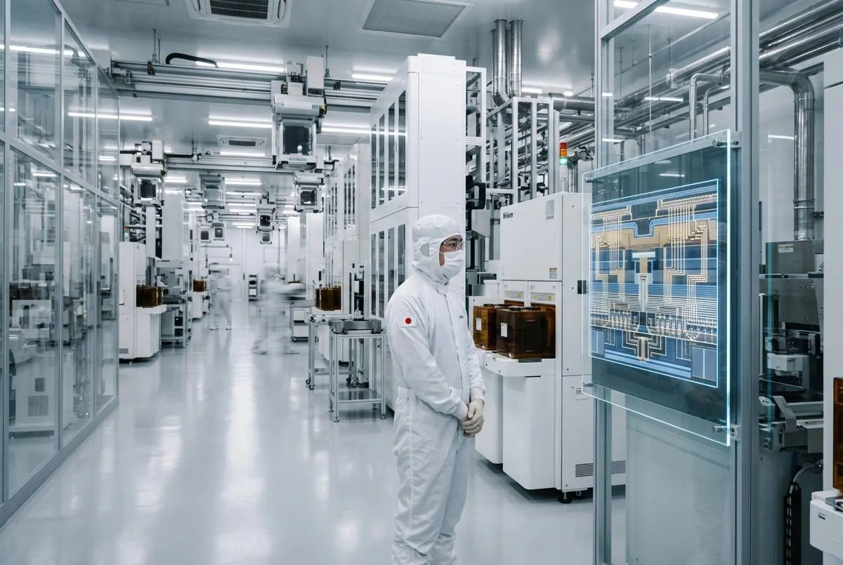
There is a complication sitting directly under the fab. Kumamoto sits in one of Japan's most seismically active regions, and a July earthquake tested the area's resilience. EUV lithography tools demand vibration-isolated foundations held to tolerances that make them acutely sensitive to seismic events; a meaningful tremor can halt production and require lengthy recalibration.
None of this is disqualifying. Taiwan itself is earthquake-prone, and TSMC's home fabs are engineered for it. But the seismic risk is one reason industry watchers treat the Fab 2 upgrade as a qualitatively different bet from Fab 1. The first fab's mature-node business rests on multi-year qualification agreements with automotive customers: demand that is structural, slow-moving, and predictable. The second fab's customers will be AI accelerator designers, hyperscalers, and advanced consumer chip teams, whose demand cycles run faster and less predictably. TSMC is trading a steady annuity for a position in the fastest-moving, highest-margin segment of the industry.
What it means for Japan's AI ambitions
Takaichi's government has promised financial support to see the plan through, and the political logic is plain. Japan has spent the better part of a decade trying to rebuild a domestic semiconductor ecosystem that once led the world and then steadily lost ground. JASM's first fab restored volume manufacturing; a 3nm AI fab would give Japan something it has not had in a generation: a front-row seat at the leading edge.
The timing is deliberate. Wei delivered the announcement just before a Japanese general election, and Takaichi called the news "thrilling" in Japanese media coverage. The two leaders framed the plant as a template for economic cooperation and a reinforcement of the global chip supply chain. For Tokyo, advanced chips made domestically answer both an industrial policy goal and an economic security one, reducing dependence on supply chains that run through a single strait.
The global balancing act
Kumamoto does not exist in isolation. It is one leg of the most ambitious fab expansion in history. TSMC is investing $165 billion in the United States, described as the largest single foreign investment in the nation's history, covering five wafer fabs, two advanced packaging plants, and a research and development center. Japan's $20 billion program, Germany's Dresden fab, and the relentless expansion in Taiwan form the rest of the map.
The through line is that leading-edge capacity has become a geopolitical asset, and every major economy wants some within its borders. The Kumamoto upgrade is TSMC's clearest signal yet that AI demand is strong enough to justify placing its crown-jewel process technology far from home. If the 2028 ramp hits its targets, Japan will be making chips that power AI servers, robots, and autonomous vehicles. If it slips, the delay will be measured not just in wafers but in the credibility of the industry's great geographic diversification. Either way, the filing this week made the stakes official.
0 Comments