
On October 12, 2026, Applied Materials officially unveiled its $5 billion EPIC Center in Sunnyvale, California, and the guest list read like the semiconductor industry's entire org chart. TSMC, Intel, Samsung, Micron, and SK hynix, five companies that spend their days trying to out-build, out-price, and out-engineer each other, signed on as founding partners. Under one roof, they will now do something they almost never do: share a research floor.
EPIC stands for Equipment and Process Innovation and Commercialization, and the name is the strategy. Applied Materials, the largest chipmaking equipment supplier in the United States, built the center to collapse the industry's oldest bottleneck: the handoff between the people who invent chipmaking processes and the people who run them at scale.
The lab that collapses the handoff
The traditional way to move a chipmaking innovation from idea to factory is a relay race. Materials researchers work in one environment. Equipment and process development happens in another. Integration and pilot production happens in a third, often on a different continent. At each handoff, months can evaporate while wafers ship back and forth between toolmakers in the United States, Europe, and Japan and fabrication plants scattered across Asia.
EPIC is designed to remove those handoffs. The center puts materials scientists, equipment engineers, and the chipmakers' own process teams in a single state-of-the-art facility purpose-built for commercialization. Partners bring their engineers and their roadmap challenges into the building and work in what Applied calls secure learning cycles alongside its teams, running early experiments on production-relevant tools rather than university-scale equipment.
The building itself is engineered to signal scale. Thirty-four roof trusses cover the cleanrooms, each spanning nearly 300 feet in length and weighing as much as twelve school buses. The facility is also designed to recycle and reuse approximately 40 percent of its water, a practical detail that matters in drought-prone California, where fabs are among the thirstiest industrial users around.
The technologies the AI era demands are too complex and too consequential for any one company to invent alone.
A year of partner assembly
Enjoying this story?
Get the five most important stories in tech, every morning. Free.
The unveiling looked like a single announcement, but the roster was assembled deliberately over the better part of a year. Samsung Electronics joined as the first founding partner in February 2026. Micron and SK hynix followed in March, completing a memory-tier cohort that includes all three of the world's largest DRAM producers. Advantest, the automated test equipment company, became the first innovation partner in April. TSMC signed as a founding partner in May, focused on advanced logic. Broadcom joined the same month as an innovation partner focused on packaging. KIOXIA, the Japanese flash manufacturer, came aboard in September. The Dutch packaging equipment maker Besi joined on October 1, and Intel's October 6 announcement capped the roster just days before the unveiling.
The sequencing reads like a map of the AI chip supply chain: memory (Samsung, SK hynix, Micron, KIOXIA), advanced logic (TSMC, Intel), packaging equipment (Besi, SCREEN), test (Advantest), and design (Broadcom). The five universities, Stanford, UC Berkeley, Arizona State, Rensselaer Polytechnic Institute, and UCLA's Samueli School of Engineering, which joined just four days before the unveiling, give academic researchers access to commercial-grade tools so their work can be tested in something close to a real fab rather than a campus cleanroom.
Why the industry is suddenly cooperating
The $5 Billion Chip Lab, in Numbers
Applied Materials' EPIC Center, unveiled October 12, 2026.
Note: For illustrative purposes only.
The timing is not an accident. Applied told investors in May that leading-edge foundry logic, DRAM, and advanced packaging should account for more than 80 percent of the year-on-year growth in total wafer fab equipment spending in 2026, and that its own packaging revenue should grow more than 50 percent this calendar year. In other words, the fastest-growing parts of the industry are exactly the parts where progress now depends on solving problems across company boundaries: a new memory design means little if the packaging that connects it to the processor cannot keep up.
The economics of AI infrastructure are driving the shift. TSMC chairman C.C. Wei noted at the unveiling that the leading-edge production node has moved from 350 nanometers three decades ago to 2 nanometers today, and that collaboration continues beyond that point toward energy-efficient AI architectures. Intel CEO Lip-Bu Tan described a path to more than a trillion transistors in a single package by 2030, a target that only makes sense if transistors, interconnects, and packaging advance together. Samsung and SK hynix each framed the center as a way to accelerate next-generation HBM, DRAM, and NAND roadmaps from early concept to fab yield.
The common thread: no single company can refine the tools, materials, and processes for the next generation fast enough on its own. Whoever shortens the cycle from lab to high-volume manufacturing wins the race, and the race is now measured in months, not years.
The catch: cooperating with your rivals
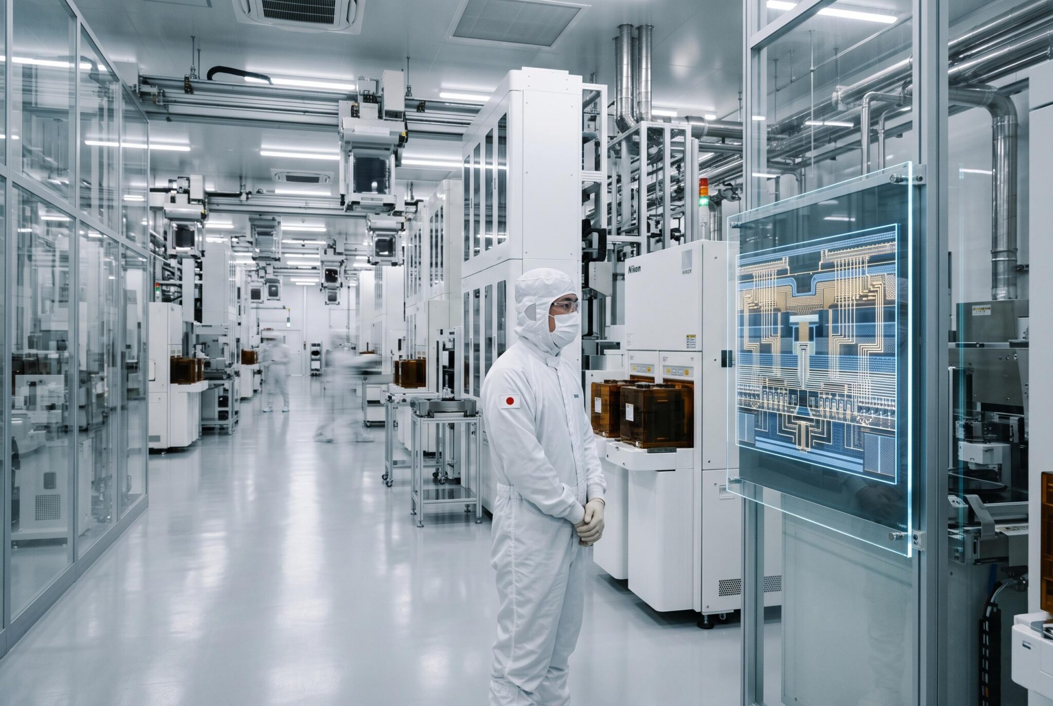
None of this changes the fact that the founding partners are competitors. TSMC and Samsung fight over the same foundry customers. Intel and TSMC are vying for leadership at the most advanced nodes. Samsung and SK hynix battle in DRAM and high-bandwidth memory. Sharing a research floor with direct rivals is a meaningful cultural shift for an industry built on secrecy.
Applied's answer is the structure of the work itself: secure learning cycles in which each partner pursues its own roadmap challenges in isolation from the others, but on shared infrastructure, alongside Applied's engineers. The competitors do not see each other's recipes. They share the kitchen.
The arrangement also deepens Applied's own position. By hosting the shared environment, the company gets early visibility into the process problems its customers will face, which lets it shape tools and services around those needs before customers lock into production schedules. It is offering a faster feedback loop while placing itself closer to the earliest process decisions in the industry. That is good for innovation, and it is very good for Applied.
What comes next
A building is not a breakthrough. The center opens now, but the process innovations it is supposed to accelerate will take years to reach high-volume manufacturing, and Applied expects additional companies to join the ecosystem over time, which means the roster announced this week is the floor, not the ceiling.
But the significance of EPIC goes beyond one company. It is one of the largest single R&D bets made in Silicon Valley in recent memory, and it codifies a theory about where chipmaking progress comes from in the AI era: not from a single genius lab or a single dominant fab, but from the messy, expensive, cooperative work of making every link in the chain advance at once. Applied just built the building where that work is supposed to happen. Now we get to see whether the industry's fiercest rivals can actually share it.
0 Comments