
For two years, the semiconductor industry's scarcest resource was logic: advanced nodes at TSMC and the wafer capacity to etch them. That era has quietly ended. The scarcest resource in chips is now memory, and the numbers are getting startling.
Contract pricing for HBM4, the sixth generation of high-bandwidth memory that sits next to every new AI accelerator, is projected to jump 121 percent year over year in 2027, according to reporting from the Korea Economic Daily this week. A 12-high, 36-gigabyte HBM4 stack would go from roughly $600 in 2026 to about $1,300 next year. On October 7, AMD chief executive Lisa Su flew to Seoul, her second trip to South Korea in seven months, to negotiate expanded memory supply with Samsung. Every AI GPU shipping next year needs HBM4, and there is simply not enough of it.
What HBM4 is, and why it is suddenly precious
High-bandwidth memory is DRAM stacked vertically, with dies connected through microscopic copper pillars called through-silicon vias and bonded under heat and pressure. The stack sits beside the accelerator die on a silicon interposer, shuttling data across a bus 2,048 bits wide, double the width of the previous generation. Samsung's implementation is rated at up to 3.3 terabytes per second of bandwidth per stack; SK hynix demonstrated a 16-layer stack packing 48 gigabytes at around 2 terabytes per second.
Mass production began in the second quarter of 2026, at the industry's biggest product transition. NVIDIA's Vera Rubin platform, the architecture succeeding Blackwell, is already in mass production and depends on HBM4. AMD has begun shipping its Instinct MI455 accelerator with 432 gigabytes of HBM4 onboard. Both companies, plus every hyperscaler building custom silicon, now draw from the same finite capacity at three suppliers: Samsung, SK hynix, and Micron.
The arithmetic of a 121 percent price jump
Enjoying this story?
Get the five most important stories in tech, every morning. Free.
The projected price spike reflects buyers bidding up scarce allocation, and scarcity is now structural. SK hynix says its HBM4 yields are nearing the previous generation's maturity, and HBM4E is already planned for mass production in 2027. Micron's CEO Sanjay Mehrotra told investors in early October that about 75 percent of the company's 2027 memory output is already sold, with conversations moved to 2028. HBM for AI accelerators now outranks even server DRAM in priority.
Every MI455 and every Vera Rubin board is a bid in the same auction. The auction is for HBM4, and the auction is rigged by physics: only three companies can sell.
The squeeze spills beyond the data center. Consumer DDR4 contract prices jumped 24 percent over the past three months and DDR5 rose 20 percent, per a Barclays analysis reported this week. The connection is direct: HBM4 and consumer DRAM come from the same fabs, wafers, and packaging engineers. When memory makers prioritize HBM4 for AI accelerators because it carries far higher margins per wafer, capacity gets pulled away from consumer lines. Intel's CEO Lip-Bu Tan delivered the industry's starkest summary earlier this year, after consulting two major memory players: "There's no relief until 2028."
Seoul's memory war: faster vs. taller
The HBM4 squeeze, in numbers
Projected pricing and market shares behind the memory crunch.
Note: Price and share figures are reported industry estimates, not company guidance.
This week the rivalry between Samsung and SK hynix was on full display at SEDEX 2026, Korea's largest semiconductor trade show, which opened Wednesday at the COEX convention center with a record 300 companies and 888 booths. The two titans set up side by side, exhibiting competing prototypes built on opposite engineering theories.
Samsung's HBM4 is built on its sixth-generation 1c DRAM process, a 10-nanometer-class node one generation ahead of its rivals, stacked 12 dies high. Running at 11.7 to 13 gigabits per pin and built over a 4-nanometer logic base die borrowed from Samsung's foundry playbook, the stack tops out near 2.8 terabytes per second. It is a bet on speed: AI training moves model weights in massive parallel bursts, and raw bandwidth is the binding constraint.
SK hynix took the other path. Its HBM4 uses a more mature 1b process, but stacks 16 dies instead of 12, reaching 48 gigabytes per stack versus Samsung's 36. The logic is about inference, not training. When a model serves long conversations, it stores a key-value cache of every previous token in memory, and that cache can balloon until it overflows the available HBM, forcing data down into slower tiers. SK hynix president Ahn Hyun made exactly this argument in his SEDEX keynote, forecasting that AI infrastructure must scale roughly 20-fold by 2030 and framing KV cache overflow as the central bottleneck. His bet: capacity, not bandwidth, will decide the next round.
Why three suppliers cannot fix this with money alone
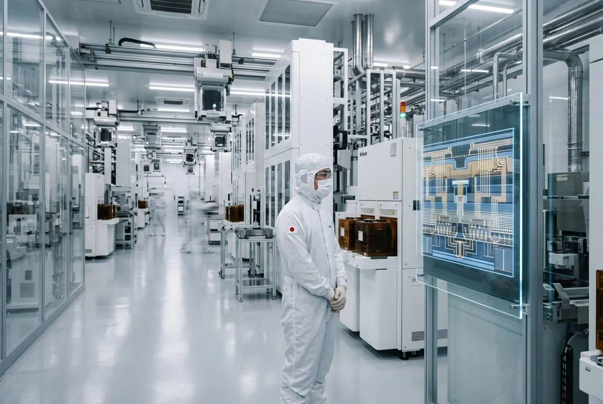
The usual cure for a shortage is capital spending, and some of that is arriving. ASML, the Dutch firm whose lithography tools the memory industry depends on, reported record quarterly net sales of 11.7 billion euros for the third quarter of 2026, with order books signaling tool purchases extending through 2030. But memory capacity has a second, slower bottleneck: the bonding equipment. Thermal compression bonders, which fuse each DRAM die into the stack, are dominated by a single Korean toolmaker, Hanmi Semiconductor. At 16-high stacking, a 97 percent per-layer yield still produces a finished stack yield below 61 percent, so every layer added multiplies the demand for bonding precision. SK hynix signed a 44.2 billion won contract with Hanmi for upgraded TC Bonder 4.5 Griffin units for its Cheongju facility, a reminder that supply is gated by equipment as much as by wafers.
There is also a strategic layer that money cannot buy: qualification. All three suppliers have passed NVIDIA's HBM4 qualification for Vera Rubin, but industry estimates still put SK hynix at 60 to 70 percent of Vera Rubin HBM4 volume and Samsung at 25 to 30 percent. Samsung has an internal target for HBM4 to exceed half of its total HBM output, and its three-year memorandum with AMD, signed around Su's visit, covers HBM4, advanced DDR5, joint development, advanced packaging, and potentially even foundry manufacturing: scarce memory as leverage to win logic orders that would otherwise go to TSMC.
What comes after the squeeze
The most interesting signal from SEDEX was the roadmap. SK hynix proposed a new memory tier, High Bandwidth Flash: a NAND-based package in an HBM-compatible form factor delivering roughly half the bandwidth of HBM4 at more than ten times the capacity per package, with the standard planned for January 2027. Its target is the same KV cache overflow problem. Alongside 3D-stacked DRAM and custom HBM with customer-specific logic in the base die, it points to a memory hierarchy with many more tiers than today's DRAM-and-flash split.
That future cannot arrive fast enough for buyers paying 121 percent more next year. But it reveals something structural about this shortage. The memory industry is not just short of wafers; it is short of architectural answers to what AI actually needs. Samsung and SK hynix disagree about the answer, which is why their HBM4 chips look so different. The market will tell them which one was right, and the price of being wrong is being measured in billions.
0 Comments